Introduction
The Arithmetic Logic Unit (ALU) is essentially the heart of a CPU. This is what allows the computer to add, subtract, and to perform basic logical operations such as AND/OR. Since every computer needs to be able to do these simple functions, they are always included in a CPU. How a company designs their ALU has a significant impact on the overall performance of their CPU. In this article I will give a brief introduction to some basics of ALU design; you will quickly see how complicated these things can get.
Logic Gates
Before we get to the overall design of an ALU, we first have to understand the basics of logic gates. Figure 1 shows the basic logic gates shown in their graphical representations. Keep in mind that each of these can be made from transistors by combining them in different ways. What types of transistors and how they are arranged can impact the performance of the gate.

‘AND’ Gate

‘OR’ Gate

‘XOR’ Gate

‘NOT’ Gate
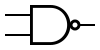
‘NAND’ Gate

‘NOR’ Gate

‘XNOR’ Gate
Figure 1: Basic logic gates (courtesy of wikipedia.com)
These logic gates work by taking two inputs (one input for the ‘NOT’ gate) and producing an output. If we consider the ‘AND’ gate the output will be true, or ‘1’ (or a high voltage), if input #1 and input #2 are true, and the output will be false, or ‘0’ (or a low voltage), if one or both inputs are false. Likewise, if we consider the ‘OR’ gate the output will be true if input #1 or input #2 are true. The ‘XOR’ gate output will be true if either input is true, but false if both inputs are true; this is an implementation of the exclusive ‘OR’ logic operation. The ‘NOT’ gate will output the opposite of the input; so if the input is true the ‘NOT’ gate’s output will be false. The ‘NAND’, ‘NOR’, and ‘XNOR’ gates are implementations of the ‘AND’, ‘OR’, and ‘XOR’ gates respectively with a ‘NOT’ gate prior to the output; so a ‘NAND’ gate will return what a ‘AND’ gate does not.
These logic functions are by themselves an important part of a CPU’s functionality, but performing logic operations on two inputs is only so useful. By combining these gates together we can have devices with more inputs. For example, in Figure 2 I have combined three ‘AND’ gates. These three ‘AND’ gates will produce an output that is true only when all four inputs are true. In essence, this is a 4 bit ‘AND’ gate. You can extrapolate from this and form an 8 bit ‘AND’ gate by combining two 4 bit ‘AND’s and one 2 bit ‘AND’.

Figure 2: A 4 bit ‘AND’ device
Arithmetic
By combining these gates into even more clever configurations we can perform other useful functions, like addition. Figure 3 shows a typical configuration referred to as a half-adder. To understand how this adder works we have to think of the inputs not as true or false but as ‘1’ or ‘0’. The output of this adder is the sum of the inputs with a carry bit. If the inputs are ‘1’ and ‘1’ we are adding 1 plus 1. The output labeled ‘SUM’ is just an ‘XOR’ of the inputs which will be ‘0’. The output labeled ‘CARRY’ is an AND gate which of course will be ‘1’. The addition answer therefore is 10 which is the binary addition of ‘1’ and ‘1’. If the inputs are ‘1’ and ‘0’ the ‘SUM’ will be ‘1’ and the ‘CARRY’ will be ‘0’, giving an answer of 01 or just 1.

Figure 3: A half-adder
So, if this is performing binary addition why is it called a half-adder? This is because in order to add binary numbers greater than two bits we need the adder to be able to take in a carry bit along with the two input bits. This full-adder is shown in Figure 4. You can see that the full-adder is two half-adders with one additional ‘OR’ gate. To use a full-adder to add two binary numbers of arbitrary size you will begin with the right most bit, called the least significant bit (LSB) of each number with a carry in bit of ‘0’. You would then add the two bits, record the sum, and use the carry out bit as the carry in bit when adding the next two bits and moving towards the most significant bits (MSB). By repeating this process you can add two binary numbers of any arbitrary length. This process is known as a ripple carry.

Figure 4: A full-adder
Figure 5 shows a half-sub. In this scenario if we have input ‘A’ equal to ‘1’ and input ‘B’ equal to ‘0’ we want to subtract 0 from 1. You can see that the ‘DIFF’ output will be ‘1’ and the ‘BORROW’ Output will be ‘0’. Like the half-adder, the half-sub can be used to implement a full-sub, shown in Figure 6.

Figure 5: A half-sub

Figure 6: A full-sub
Arithmetic units are usually grouped together into an ALU which has inputs, outputs, and control bits which tell the ALU which type of operation to perform. Figure 7 shows a typical diagram of an ALU. In this diagram A and B are the data inputs, F is the control input to choose the function, R is the result of the function applied to A and B, and D is the status of the output so that you know when the function is done.

Figure 7: a typical ALU (symbol courtesy of wikipedia.com)
Optimizations
The example of the ripple carry addition is an effective method of adding binary numbers. Let us extrapolate this a little bit and imagine a 32-bit adder. If we want to add two 32-bit numbers we can start at the LSB and move left as we calculate the carry bits. If adding two bits takes a couple of clock cycles, then the total time taken to add all 32 bits is significant. Thankfully this problem has already been solved. The solution: a carry look ahead adder.
In a carry look ahead adder the binary numbers are split into sections, perhaps of 4 bits each. Now each section can begin calculating its carry bits beginning with the section’s LSB and moving towards the section’s MSB. Once a carry bit reaches the MSB of its section the bit can then jump ahead 4-bits at a time instead of continuing towards the number’s MSB one bit at a time. The logic involved with keeping all of the carries straight is quite complex and becomes more complex as the size of the sections increase; because of this more time is spent calculating the carries of each section and less time on the faster propagation of the carry bits. However, if the section size is too small then there are so many sections for the carries to propagate through that there is not much time saved versus the ripple carry adder. Deciding upon a section size involves a detailed analysis of the gate and propagation delays which can vary depending on the technology used within the logic gates.
The carry look ahead technique is one optimization the engineers can make to the ALU. There are many others. For instance, to do multiplication one would normally just add the number to itself over and over, but there are optimization techniques that can be employed to speed this process up. These are some of the differences between the ALUs of various processors and a major reason why some processors are better at certain types of operations than others. For instance, a GPU will have an ALU which is optimized for the arithmetic often performed for the display of graphics while a CPU will have an ALU designed to be optimized for the most common operations performed by users.